The artificial intelligence revolution has necessitated a fundamental reimagining of computational hardware, moving beyond traditional CPUs and GPUs to purpose-built silicon architectures designed specifically for machine learning workloads. Three groundbreaking approaches have emerged as leaders in this domain: Google’s Tensor Processing Units (TPUs), Tesla’s Dojo supercomputing platform, and Cerebras Systems’ revolutionary Wafer-Scale Engine. Each represents a distinct philosophical approach to solving the computational challenges inherent in training and deploying large-scale neural networks, offering unique advantages and trade-offs that make them suitable for different aspects of the AI ecosystem.
Explore the latest AI hardware trends to understand how custom silicon is reshaping the boundaries of what’s possible in artificial intelligence computation. The convergence of specialized hardware design, advanced manufacturing processes, and innovative architectural approaches has created a new competitive landscape where traditional semiconductor companies must compete alongside technology giants who have ventured into custom chip design to optimize their AI workloads.
The Evolution of AI-Specific Computing
The transition from general-purpose computing to AI-specific silicon represents one of the most significant architectural shifts in semiconductor design since the introduction of graphics processing units. Traditional processors were designed for versatility, capable of handling a wide variety of computational tasks with reasonable efficiency. However, the mathematical operations fundamental to neural network training and inference follow predictable patterns that can be dramatically accelerated through specialized hardware architectures optimized for matrix multiplication, tensor operations, and the specific data flow patterns characteristic of deep learning algorithms.
This specialization has enabled performance improvements measured not in percentage gains but in orders of magnitude, fundamentally changing the economics of AI research and deployment. Where previously training large language models or computer vision systems required months of computation time on traditional hardware, custom AI silicon has compressed these timelines to weeks or even days, while simultaneously reducing energy consumption and operational costs. The implications extend far beyond mere performance improvements, enabling entirely new categories of AI applications that were previously computationally infeasible.
Google TPU: Pioneering Tensor Processing Architecture
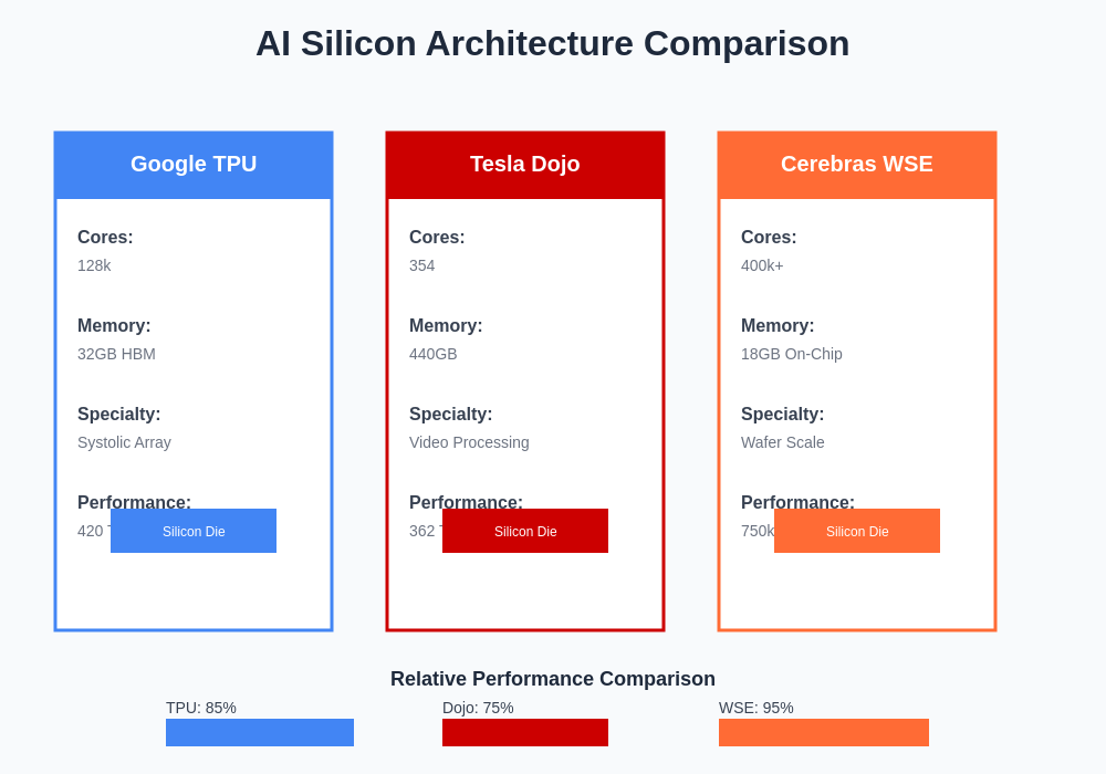
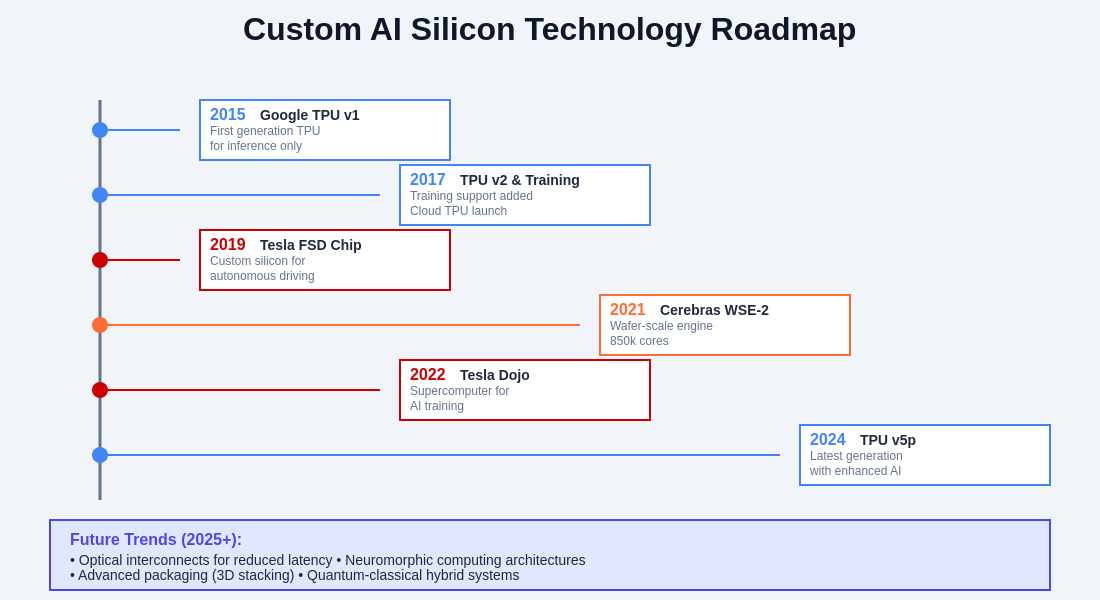
Google’s Tensor Processing Units represent the most mature and widely deployed custom AI silicon ecosystem, having evolved through multiple generations since their initial deployment in 2015. The TPU architecture fundamentally reimagines the computational pipeline for machine learning workloads, featuring a systolic array design that optimizes data flow for matrix multiplication operations central to neural network computation. This approach eliminates many of the inefficiencies inherent in adapting general-purpose processors for AI workloads, achieving remarkable improvements in both performance per watt and raw computational throughput.
Experience advanced AI capabilities with Claude to understand how optimized hardware architectures enable more sophisticated AI applications and faster model development cycles. The TPU ecosystem encompasses not just the processing units themselves but an entire software stack including TensorFlow integration, distributed training frameworks, and cloud-based deployment infrastructure that has democratized access to high-performance AI computing for organizations of all sizes.
The architectural innovations embodied in TPUs extend beyond simple performance optimization to address fundamental challenges in AI system design. The systolic array architecture enables predictable data movement patterns that minimize memory bandwidth bottlenecks, while specialized numeric formats optimized for neural network computation allow for higher computational density without sacrificing model accuracy. The result is a computing platform that can train models with billions of parameters while maintaining energy efficiency levels impossible to achieve with traditional hardware architectures.
The fundamental architectural differences between these three approaches reflect distinct optimization priorities and design philosophies. Each platform demonstrates unique strengths that make them particularly well-suited for different categories of AI workloads and deployment scenarios.
Tesla Dojo: Revolutionizing Autonomous Vehicle AI Training
Tesla’s Dojo supercomputer represents perhaps the most ambitious custom silicon project undertaken by a non-semiconductor company, designed specifically to address the unique computational requirements of autonomous vehicle development. Unlike general-purpose AI accelerators, Dojo has been architected from the ground up to handle the massive video datasets generated by Tesla’s fleet of vehicles, requiring capabilities that span computer vision, sensor fusion, and real-time decision-making algorithms that must operate with extraordinary reliability and safety margins.
The Dojo architecture embodies Tesla’s vertical integration philosophy, combining custom silicon design with proprietary neural network architectures and training methodologies developed specifically for autonomous driving applications. This holistic approach enables optimizations that would be impossible to achieve through general-purpose hardware, including specialized data paths for processing multiple simultaneous video streams, dedicated circuits for sensor fusion algorithms, and memory hierarchies optimized for the temporal data patterns characteristic of driving scenarios.
What distinguishes Dojo from other AI accelerators is its focus on handling the entire autonomous driving pipeline within a unified computational framework. Traditional approaches require multiple specialized processors for different aspects of the autonomous driving task, creating latency bottlenecks and synchronization challenges that can compromise safety-critical decision-making. Dojo’s integrated approach eliminates these architectural compromises while achieving the computational scale necessary to process petabytes of driving data for continuous model improvement and validation.
Cerebras Wafer-Scale Engine: Redefining Silicon Integration
Cerebras Systems has taken perhaps the most radical approach to AI silicon design with their Wafer-Scale Engine, which utilizes an entire silicon wafer as a single integrated processor rather than cutting it into individual chips. This approach enables unprecedented computational density and memory bandwidth while eliminating the interconnect bottlenecks that limit the scalability of traditional multi-chip systems. The result is a processor containing over 400,000 cores and 18 gigabytes of on-chip memory, representing a fundamental departure from conventional semiconductor design principles.
The wafer-scale approach addresses one of the primary limitations in training large neural networks: memory bandwidth and interconnect latency. Traditional systems require complex networking infrastructures to connect multiple processors, introducing latency and bandwidth limitations that can significantly impact training efficiency. By integrating massive computational resources within a single wafer, Cerebras eliminates these bottlenecks while providing uniform, high-speed access to distributed memory resources across the entire processor.
The implications of wafer-scale integration extend beyond raw performance metrics to enable entirely new approaches to neural network training and deployment. The massive on-chip memory capacity allows for training techniques that would be impossible on traditional hardware, while the uniform computational fabric enables novel parallelization strategies that can accelerate training for specific types of neural network architectures by orders of magnitude.
Discover comprehensive AI research capabilities with Perplexity to explore the technical innovations and research methodologies that have enabled these breakthrough silicon architectures. The convergence of advanced manufacturing processes, novel architectural approaches, and specialized software ecosystems represents a new paradigm in computing that extends far beyond traditional semiconductor design principles.
Architectural Philosophies and Design Trade-offs
Each of these custom AI silicon approaches embodies distinct architectural philosophies that reflect different priorities and use case requirements. Google’s TPU design prioritizes versatility and ecosystem integration, enabling deployment across a wide range of machine learning applications while maintaining compatibility with popular frameworks and development tools. This approach maximizes accessibility and adoption but may sacrifice some performance optimization opportunities available through more specialized architectures.
Tesla’s Dojo represents the opposite extreme, optimizing every aspect of the design for a specific application domain at the potential cost of general-purpose applicability. This specialization enables performance levels that would be unattainable through more general-purpose designs but limits the platform’s utility for applications outside the autonomous vehicle domain. The trade-off reflects Tesla’s unique position as both a hardware developer and end user, enabling design decisions that prioritize ultimate performance over broad market appeal.
Cerebras occupies a unique position in this spectrum, pursuing architectural innovations that enable new categories of computational approaches rather than simply optimizing existing paradigms. The wafer-scale approach enables capabilities that are impossible to achieve through conventional architectures but requires fundamental changes in software development methodologies and system design principles. This approach offers the potential for breakthrough performance improvements but demands significant investment in new development tools and programming paradigms.
Performance Characteristics and Benchmarking
Comparing performance across these diverse architectures presents significant challenges due to fundamental differences in design philosophy, target applications, and optimization priorities. Traditional benchmarking approaches developed for general-purpose processors fail to capture the nuanced trade-offs inherent in specialized AI silicon, requiring new evaluation methodologies that consider factors such as memory bandwidth utilization, energy efficiency, and application-specific throughput characteristics.
Google TPUs demonstrate exceptional performance in distributed training scenarios, particularly for large language models and recommendation systems that benefit from the systolic array architecture’s optimization for matrix multiplication operations. The TPU ecosystem’s maturity enables deployment at massive scale with proven reliability and software integration, making it the preferred platform for many production AI applications that require both high performance and operational stability.
Tesla Dojo’s performance characteristics are difficult to evaluate objectively due to the proprietary nature of both the hardware and the applications for which it has been optimized. However, Tesla’s reported improvements in training efficiency for autonomous driving models suggest performance levels that significantly exceed what would be achievable through general-purpose hardware, validating the benefits of application-specific optimization despite the associated development complexity and cost.
Cerebras Wafer-Scale Engine demonstrates unprecedented performance for specific categories of neural network architectures that can effectively utilize the massive on-chip memory and uniform computational fabric. Training tasks that traditionally require distributed computing approaches across multiple processors can often be executed more efficiently on a single Cerebras system, dramatically simplifying software development while achieving superior performance for compatible workloads.
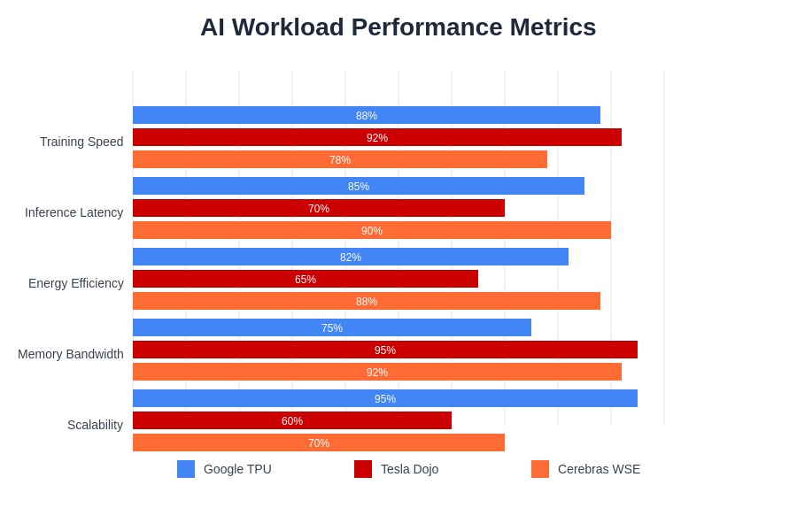
The performance characteristics of each architecture reveal distinct optimization patterns that align with their intended use cases. These metrics demonstrate how architectural choices directly translate into measurable performance advantages for specific types of AI workloads.
Manufacturing Complexity and Economic Considerations
The manufacturing requirements for custom AI silicon introduce complexity and cost considerations that extend far beyond traditional semiconductor production. Each architecture requires specialized manufacturing processes, testing methodologies, and yield optimization techniques that reflect the unique design requirements and performance targets of AI-specific computing applications. These manufacturing challenges directly impact the economics of AI hardware development and deployment, influencing adoption patterns and market dynamics.
Google’s TPU manufacturing leverages established semiconductor fabrication processes while incorporating design optimizations that maintain compatibility with high-volume production techniques. This approach enables cost-effective manufacturing at scale while ensuring consistent performance and reliability characteristics across production batches. The manufacturing approach reflects Google’s priority on widespread deployment and ecosystem development rather than pushing the absolute boundaries of semiconductor process technology.
Tesla’s Dojo manufacturing represents a more experimental approach, incorporating novel packaging technologies and system integration techniques that enable the unique architectural characteristics required for autonomous vehicle training workloads. The manufacturing complexity reflects the specialized nature of the application, with production volumes and cost optimization taking secondary priority to achieving the performance characteristics necessary for Tesla’s autonomous driving development program.
Cerebras faces perhaps the most significant manufacturing challenges due to the wafer-scale integration approach, which requires perfect or near-perfect yield across an entire silicon wafer. Traditional semiconductor manufacturing accepts a certain percentage of defective areas within each wafer, with functional chips selected and packaged for sale. Cerebras must achieve functionality across the entire wafer surface, requiring advanced yield optimization techniques and fault tolerance mechanisms that represent significant innovations in semiconductor manufacturing methodology.
Software Ecosystem and Development Tools
The success of custom AI silicon extends far beyond hardware performance characteristics to encompass the software ecosystems, development tools, and programming frameworks that enable developers to effectively utilize these specialized computing platforms. Each architecture requires unique software abstractions and development methodologies that can present significant barriers to adoption while simultaneously enabling performance optimizations impossible to achieve through traditional software development approaches.
Google has invested extensively in creating a comprehensive software ecosystem around TPUs, including tight integration with TensorFlow, specialized compilers for optimizing neural network computation graphs, and cloud-based development environments that simplify the deployment of AI applications on TPU hardware. This ecosystem approach has been critical to TPU adoption, enabling developers to leverage specialized hardware capabilities without requiring deep expertise in custom silicon programming techniques.
Tesla’s approach to software ecosystem development reflects their vertical integration strategy, developing proprietary tools and frameworks optimized specifically for autonomous vehicle applications. While this approach limits general-purpose applicability, it enables optimizations and capabilities that would be impossible to achieve through general-purpose development tools, supporting Tesla’s unique requirements for safety-critical AI applications in automotive environments.
Cerebras has developed novel programming paradigms and development tools that can effectively utilize the unique capabilities of wafer-scale architecture. These tools require developers to rethink fundamental assumptions about parallel computing and memory management but enable performance characteristics that justify the additional complexity for applications that can benefit from the wafer-scale approach’s unique capabilities.
Energy Efficiency and Thermal Management
Energy efficiency represents a critical consideration in AI hardware design, particularly for large-scale training applications that can consume enormous amounts of electrical power. Each custom silicon architecture employs different strategies for optimizing energy efficiency while managing the thermal challenges associated with high-density computation. These considerations directly impact deployment costs and operational feasibility, particularly for organizations operating AI systems at scale.
Google TPUs achieve remarkable energy efficiency through architectural optimizations that minimize unnecessary data movement and computational overhead. The systolic array design enables predictable power consumption patterns that facilitate thermal management while achieving performance per watt characteristics that significantly exceed general-purpose processors. This energy efficiency has been critical to Google’s ability to deploy AI services at global scale while maintaining reasonable operational costs.
Tesla Dojo’s energy efficiency characteristics reflect the specific requirements of autonomous vehicle training workloads, optimizing for the computational patterns and data access requirements characteristic of computer vision and sensor fusion applications. The specialized architecture enables efficient processing of the massive datasets generated by Tesla’s vehicle fleet while maintaining thermal characteristics compatible with data center deployment requirements.
Cerebras Wafer-Scale Engine faces unique thermal management challenges due to the concentrated computational density within a single wafer-scale processor. However, the elimination of inter-chip communication overhead and the uniform thermal distribution across the wafer surface enable cooling strategies that can achieve competitive energy efficiency despite the concentrated heat generation. The approach requires sophisticated thermal management systems but can achieve overall energy efficiency improvements through the elimination of traditional multi-chip system overhead.
Market Impact and Industry Adoption
The introduction of custom AI silicon has fundamentally altered the competitive dynamics of both the semiconductor industry and the artificial intelligence sector. Traditional semiconductor companies must now compete with technology companies that have developed specialized AI hardware capabilities, while AI researchers and practitioners must navigate an increasingly complex landscape of hardware options with distinct performance characteristics and optimization requirements.
Google’s TPU ecosystem has achieved the broadest market penetration, enabling organizations across various industries to access high-performance AI computing capabilities through cloud-based services. This accessibility has democratized advanced AI capabilities while creating new competitive pressures for organizations that must now compete with entities having access to state-of-the-art AI infrastructure. The TPU ecosystem’s success has validated the market demand for specialized AI hardware while establishing new expectations for AI system performance and capabilities.
Tesla’s Dojo represents a different model of custom silicon development, where the hardware developer is also the primary end user. This approach enables optimizations and capabilities that would be difficult to achieve through general-purpose hardware but limits the broader market impact to competitive pressures within the autonomous vehicle industry. Tesla’s success with custom silicon has inspired other companies to consider vertical integration strategies for critical AI applications.
Cerebras has focused on enabling breakthrough capabilities for specific types of AI research and development, particularly applications that benefit from the unique characteristics of wafer-scale integration. While the market adoption has been more limited compared to TPUs, Cerebras has demonstrated the viability of radical architectural innovations in AI hardware design, influencing broader industry thinking about the possibilities for specialized AI computing platforms.
Future Implications and Technology Roadmaps
The success of custom AI silicon has established new trajectories for both semiconductor technology development and artificial intelligence research, with implications that extend far beyond the immediate performance benefits of specialized hardware. The convergence of advanced manufacturing capabilities, novel architectural approaches, and sophisticated software ecosystems suggests that custom AI silicon will continue to drive innovation in both hardware and software domains for the foreseeable future.
Google’s TPU roadmap indicates continued evolution toward more flexible and capable architectures that can efficiently handle emerging AI workloads while maintaining the ecosystem integration that has driven widespread adoption. Future generations are expected to incorporate emerging technologies such as optical interconnects and novel memory architectures while extending support for new categories of machine learning algorithms and deployment scenarios.
Tesla’s investment in Dojo represents a long-term commitment to custom silicon development that reflects their strategic priorities in autonomous vehicle development. The platform’s evolution will likely continue to focus on the specific requirements of autonomous driving applications while potentially expanding to related areas such as robotics and other embodied AI applications that share similar computational characteristics and safety requirements.
Cerebras continues to push the boundaries of wafer-scale integration while developing new applications and use cases that can benefit from their unique architectural approach. The company’s roadmap suggests continued innovation in wafer-scale technology while expanding the software ecosystem to support a broader range of AI research and development applications.
The broader implications of custom AI silicon development extend to fundamental questions about the future of computing architecture and the relationship between hardware and software optimization. As AI applications continue to evolve and new categories of machine learning algorithms emerge, the demand for specialized computing platforms will likely continue to grow, driving further innovation in custom silicon design and manufacturing techniques.
The evolution of custom AI silicon represents a convergence of advanced manufacturing capabilities, innovative architectural approaches, and sophisticated software ecosystems that will continue to drive breakthroughs in artificial intelligence capabilities and applications. The trajectory of these technologies suggests even more revolutionary developments in the coming years as the boundaries between hardware and software optimization continue to blur.
Disclaimer
This article is for informational purposes only and does not constitute professional advice. The views expressed are based on publicly available information about AI hardware technologies and their applications. Readers should conduct their own research and consider their specific requirements when evaluating AI hardware solutions. Performance characteristics and capabilities may vary depending on specific use cases, workload requirements, and implementation details. The rapidly evolving nature of AI hardware technology means that specific technical details and performance comparisons may change as new generations of these platforms are released.